Coherent in Semiconductor Manufacturing: Advanced Packaging
Coherent lasers and materials power some of the newest and most demanding back-end processes.
October 17, 2024 by Coherent
The incredible level of miniaturization we’re now seeing in microelectronics devices is due to two factors. The first is that the transistors and other components that comprise an integrated circuit chip are getting progressively smaller – a trend often called Moore’s Law.
The second is that novel techniques are being used to package individual chips together at ever increasing densities. Quite a variety of methods are currently being employed for this purpose, such as System-in-Package (SiP), 3D Packaging, 2.5D Packaging, Fan-Out Wafer-Level Packaging (FOWLP), Flip-Chip Packaging, Multi-Chip Modules (MCM), and much more. Collectively, these are called “advanced packaging” techniques. Advanced packaging enables us to make small, powerful products like smartphones.
Advanced packaging methods are more complex and difficult to manufacture than traditional “back-end” (integrated circuit packaging) techniques. One reason is that they typically involve much higher density and smaller pitch (spacing) interconnects and more intricate part structures. This translates into the need to maintain tighter mechanical tolerances on smaller parts throughout the entire back-end production process.
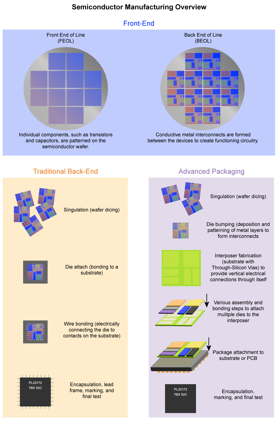
Semiconductor manufacturing is usually divided into front-end and back-end processes. And front-end is further divided into “front end of line” and “back end of line.” This illustrates the major steps in front-end and back-end processing and highlights the additional complexity of one of the many new advanced packaging methods for back-end production.
Another issue is an increased need for thermal management. The greater computational capabilities result in higher thermal design power. This means that the advanced packaging warrants the introduction of high thermal conductivity materials with high mechanical strength. High mechanical strength is needed to prevent any buckling from the weight of the multiple chips.
Lasers deliver a unique combination of precision, versatility, and efficiency for materials processing. For back-end tasks, in particular, their ability to perform non-contact processing with minimal heat affected zone is critical to creating the very small features the most advanced assembly methods depend upon. Plus, lasers are compatible with nearly any material and are even capable of processing some substances that are nominally transparent at the laser wavelength.
All this means that as packages get smaller and more complex, laser processing becomes increasingly beneficial to manufacturers. Here we will review just a few examples of the current and developing trends in laser processing for semiconductor back-end manufacturing.
Cutting and Drilling
Cutting and drilling is performed extensively throughout both traditional back-end and advanced packaging production. Some of these tasks include:
Via drilling: The creation of through holes or blind holes in printed circuit boards (PCBs) and other substrates.
Singulation: Cutting a finished wafer into individual chips.
Depaneling: Separating individual circuit boards or components from a larger panel or sheet.
Debonding: Separating components after temporary bonding processes, such as when a wafer or die has been attached to a carrier substrate for stability during thinning, processing, or handling.
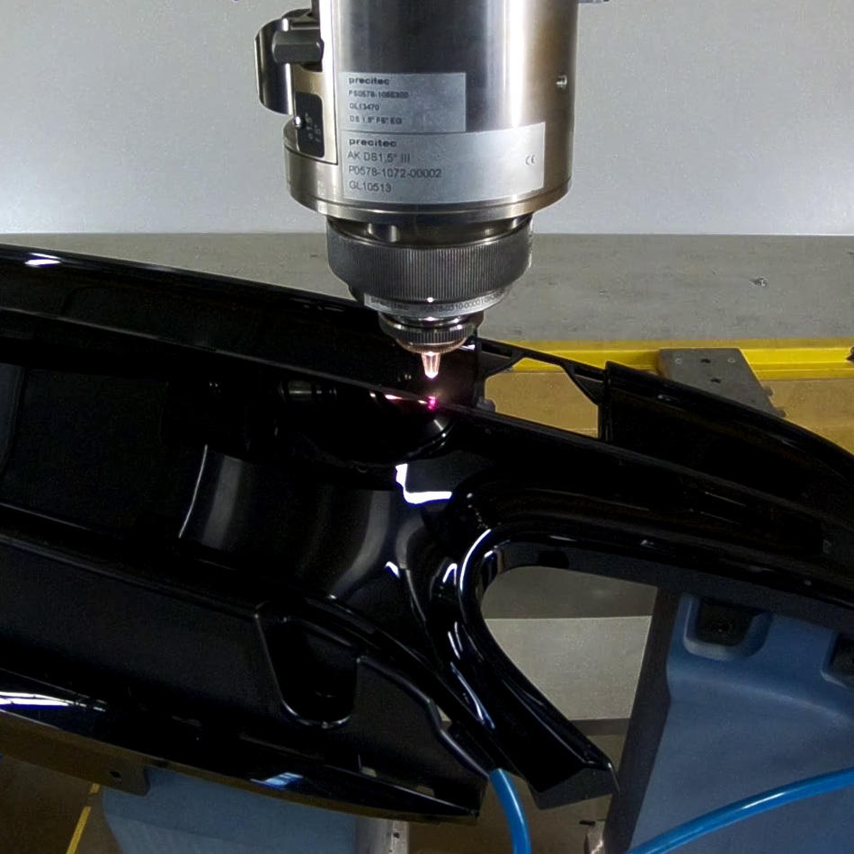
Composite materials like FR-4 (and versions of it containing woven glass fabric) and other organics have been the standard substrates for PCBs for decades. Traditionally, vias have been produced in these materials using mechanical drilling. But this method can’t produce hole diameters much below 150 µm.
Via drilling with CO₂ lasers enables high-speed drilling of vias down to 30 µm in diameter. As a result, the industry is increasingly adopting them to support the greater levels of miniaturization required for the advanced packaging techniques used in products like smartphones, 5G transceivers, and wearables. CO₂ lasers can efficiently process most of the substrates currently used, including FR4, PTFE, glass-woven composites, and ceramics.
One important recent technological breakthrough at Coherent is our Electro-optic Switch for CO₂ lasers. This modulator can handle much higher laser power than the acousto-optic modulators (AOMs) traditionally used in CO₂ laser-based drilling systems. Using a higher power laser allows the beam to be split a larger number of times. This means more holes can be drilled simultaneously which increases system throughput and reduces cost.
Coherent has also developed a proprietary spatter and debris resistant coating for via drilling windows. This multilayered coating can be placed on many different substrates. This coating is specifically developed to be frequently cleaned and stand up to metal and other debris spatter during via drilling, cutting or other marking applications. The durability of the coating also helps to extend the lifetime of the window.
This coating uses the company’s proprietary DOC (Diamond Over Coat) coating technology. The debris windows maintain high transmission and low reflection for good optical performance of the system, with an extra benefit of durability.
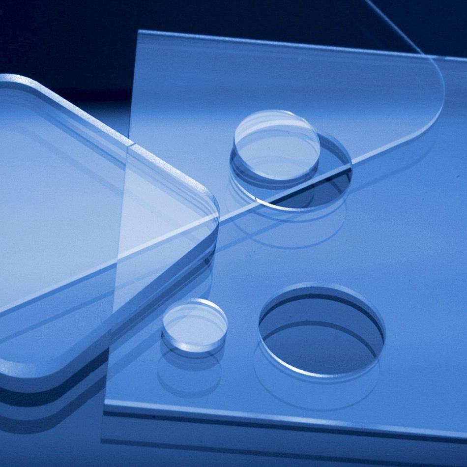
Advanced packaging methods extend the range of substrate materials well beyond FR-4 to include silicon, glass, ceramics, Ajinomoto Build-up Film (ABF), and others. CO₂ laser drilling is still the best choice for some materials like ABF, but other lasers may be more appropriate for other materials such as glass.. Plus, the required via sizes can be much smaller – as low as 10 µm or less.
Various nanosecond pulsed solid-state lasers, such as our AVIA LX and AVIA NX, can be utilized to produce these smaller vias. For the most demanding tasks, our ultrashort-pulse (USP) lasers can create extremely small holes or other features without damaging surrounding heat sensitive circuitry. Also, USP lasers – especially with ultraviolet (UV) output – are compatible with nearly any material, including metals, semiconductors, composites, ceramics, and organics.
These same nanosecond and USP lasers are also useful for other materials processing tasks, such as wafer scribing and dicing, and PCB depaneling. Here they bring the benefits of high mechanical precision, minimum kerf width, small heat affected zone, and little or no debris production along with compatibility with numerous different substrate materials. They are also compatible with substrates for next-generation advanced packaging – like glass – which have yet to be commercially deployed.
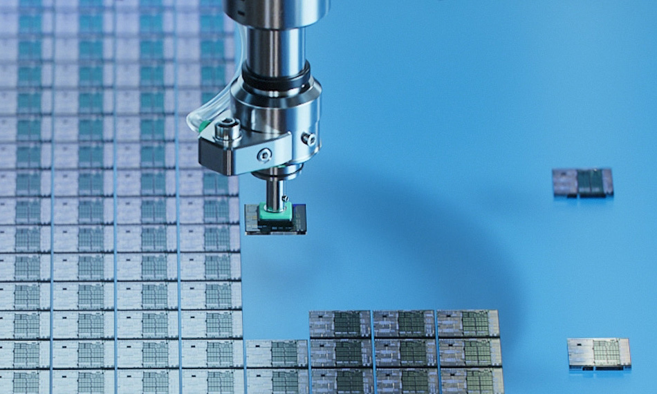
Besides lasers, Coherent also supplies innovative materials for the construction of back-end tools. For example, metal matrix composites combine the strength of steel with the lightness of aluminum, providing the necessary rigidity and thermal conductivity essential for high-performance, fast-operating robotic systems. Ensuring that equipment can operate at higher speeds without compromising accuracy is particularly important as the industry pushes towards faster production cycles. These are required to meet the increasing consumer demand for electronic devices like smartphones and computers.
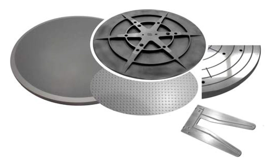
Semiconductor back end of line wafer handling components.
Marking
The spectrum of marking tasks utilized in back-end production is too extensive to detail here exhaustively. Following is an abbreviated listing of some of the most common marking applications in back-end.
Encapsulated devices: |
The most commonly used encapsulation molding compounds absorb near infrared (IR) light well and this transforms them from black into gray. This enables high contrast marks which have a depth of 30 µm to 50 µm. This type of marking is usually performed with either fiber or diode-pumped, solid-state lasers. Dual head configurations help marking trays more efficiently. |
Thin encapsulation: |
Small form factor devices, which use thin mold compound caps to protect wire bonded silicon dies, require a marking depth of 10 µm or less. Green light is more strongly absorbed than IR by the epoxy matrix, and therefore produces a shallower mark. Green lasers – usually frequency doubled fiber or diode-pumped, solid-state lasers – are used for these tasks. Our PowerLine E Twin combines high throughput by utilizing two laser sources with the advantages of DPSS laser technology. |
Ceramics: |
Ceramics are extensively used in packaging power semiconductors, high-brightness LEDs, RF devices, MEMS, hybrid circuits, and more, due to their excellent thermal, mechanical, and electrical properties. But the process window for marking ceramics is relatively narrow. This makes accurate focus and high pulse energy critical to ensuring reliable marking results. DPSS lasers based on Nd:YVO₄, offer high pulse energies , are useful for marking ceramic lids and substrates. Our PowerLine F 20-1064, which offers adjustable pulse widths up to 350 ns, is specifically designed to improve the process window for marking applications of this type. |
PCBs: |
PCBs are often marked during production with traceable data matrix codes, and the thin green solder resist layer on top of the organic substrate needs to carry the mark without exposing the copper underneath. Since data matrix codes can be quite small (with cell sizes under 125 µm), a focused laser spot size of less than 100 µm is required. Green diode-pumped, solid-state lasers have become the standard for these applications, with UV lasers such as PowerLine E 20-355 employed for marking on high-end substrates due to their finer resolution and lower thermal impact. |
Metal lids and leadframes: |
Near IR fiber lasers, including the Coherent PowerLine F Series, are widely used for marking metal lids on microprocessors and other high power consumption ICs. Metal leadframes, which are typically plated with tin, silver or gold, can be marked either before or after plating. Leadframes are used for cost sensitive devices, which makes minimizing capital investment essential. Economical fiber laser makers are often chosen for this reason. |
Thermal Compression Bonding
One of the most widely used advanced packaging techniques is “flip chip.” A critical step in the flip chip process is soldering a die to a substrate. Specifically, this involves melting metal solder bumps – which have been previously deposited onto conductive pads on the dies – while simultaneously pressing the die and substrate (usually a PCB) together.
This process becomes more challenging as both ICs and substrates get thinner, and as the solder bump sizes and spacings between them (called the pitch) shrinks below 100 µm. Thermal compression bonding (TCB) has emerged as an alternative to the traditional solder “reflow” method for flip chip applications. TCB delivers more reliable bonds and greater unit-to-unit consistency for very thin and dense substrates.
TCB equipment utilizes a plate (called a nozzle) that presses down on the die/substrate assembly during bonding. This plate must remain rigid, smooth, and flat throughout the entire bonding process. This is necessary to maintain the flatness of the die itself which, in turn, ensures that there will be no solder voids.
This nozzle must also have holes for airflow so that it can function as a vacuum chuck. Plus, it must be thermally conductive to allow the heating and cooling elements in the TCB system to control die temperature during the process.
The ideal nozzle material must therefore be mechanically rigid, and capable of being fabricated into parts that are both very smooth and flat. It must also have high thermal conductivity.
Coherent produces three materials that meet these requirements – reaction-bonded silicon carbide (SiC), single-crystal SiC, and polycrystalline diamond. Each has its own specific characteristics and advantages for certain TCB implementations.
Furthermore, Coherent is a vertically integrated TCB nozzle manufacturer. We grow each of these materials and can process them into finished parts. Plus, our metrology capabilities enable us to ensure nozzle flatness which is critical in this application.
Empowering Precision and Performance
As semiconductor packages continue to shrink and become more complex, the role of advanced laser and materials technologies becomes increasingly crucial. At Coherent, we’re committed to delivering cutting-edge solutions that enable the future of semiconductor manufacturing. Explore our comprehensive range of lasers and materials to discover how we can help you stay ahead in this rapidly evolving industry.