Coherent in Semiconductor Manufacturing: Wafer Inspection
UV lasers from Coherent enable detection of minute defects on semiconductor wafers which is key to maximizing yields and lowering cost.
October 17, 2024 by Coherent
The Apollo Guidance Computer (AGC) used by NASA for the moon landing cost approximately $150 million when it was built in the 1960s ($1 billion in today’s dollars). It was about the size of a microwave oven and weighed around 32 kg.
Today, a top-of-the-line iPhone 15 costs $1600 and, of course, fits in the palm of your hand. And that iPhone is around 200 million times more powerful than the AGC in terms of the number of operations it can perform per second.
This increase in microprocessor power was predicted by Intel co-founder Gordon Moore, who stated that the number of transistors on a microchip would double approximately every two years. But the comparison just cited also highlights an important corollary to Moore’s Law, sometimes called Moore’s Second Law. Namely, that the amount of microprocessor power available per dollar also increases exponentially over time.
Both Moore’s First and Second Laws have remained true over time because the semiconductor industry has simultaneously focused on achieving two different goals. The first is to make circuit elements and assemblies smaller. The second is to relentlessly lower costs.
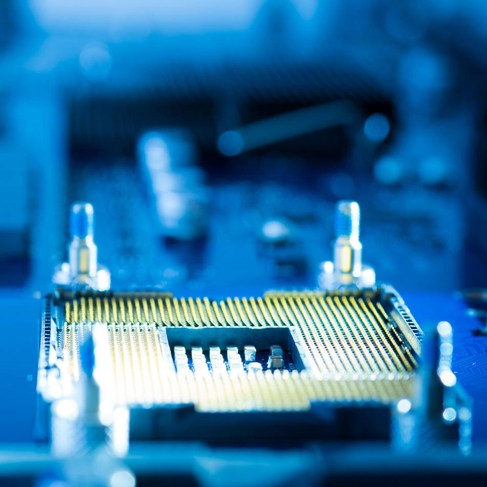
A critical cost factor in semiconductor fabrication is yield, and one significant factor affecting that is defects and contaminants in the production environment. To reduce defects, manufacturers make substantial investments in equipment, such as cleanroom environments, to prevent contamination from the outset. Additionally, they deploy advanced inspection techniques to detect and minimize the impact of any defects that do occur, ensuring optimal yields and cost efficiency.

Lasers in Wafer Inspection
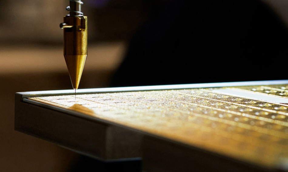
Lasers are an ideal tool for semiconductor inspection because they are a non-contact method that offers an unrivalled combination of sensitivity and speed. Furthermore, they’re highly versatile and can be optimized to perform a variety of different inspection tasks.
As a result, lasers have been used for inspection since the very early days of the microelectronics industry. In the late 1960s – not long after lasers were first introduced into the market – they were already being employed for metrology tasks, such as measuring wafer flatness and thickness.
In the 1980s, as semiconductor devices became smaller and more complex, the industry began to adopt other laser-based inspection methods. These techniques involved directing a laser beam onto the wafer surface and analyzing the returned light to detect defects, such as particles, scratches, and pattern deviations. This period saw the development of more sophisticated laser-based inspection systems, capable of detecting increasingly smaller defects critical to the production of high-quality semiconductors.
The next few decades marked significant improvements in laser-based methods, with the introduction of scatterometry and other advanced metrology techniques. Scatterometry, which uses lasers to analyze the patterns of light reflected from a wafer's surface, enabled the detection of subtle defects that were previously undetectable.
Why Small Circuits Create a Big Challenge for Inspection
Wafer inspection becomes increasingly crucial and challenging with every new generation of chips. This is because with each reduction in node size, the chip architecture becomes more complex, incorporating new materials and smaller, more intricate features. These advancements, while pushing performance boundaries, introduce new opportunities for defects to occur. And when working at such a small scale, even the smallest, most minor defect in the wafer can lead to a non-functional chip.
Therefore, manufacturers must perform rigorous inspection after key process step to catch defects early on. Performing these inspections helps optimize yield (usable chips per wafer), throughput (production speed), and, ultimately, profitability.
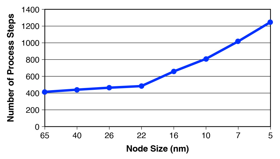
Smaller circuit features have dramatically increased the need for inspection, which is often best performed with lasers.
But a key concept to understand here is that it requires shorter wavelength lasers to push the boundaries of defect detection. This is because the efficiency of light scattering depends on the relationship between the wavelength of the light and the size of the features or defects being inspected. When the feature size is much smaller than the wavelength of the light, scattering becomes less efficient, and the signal from these features or defects diminishes. This means the defects can’t be detected – at least not on timescales relevant for high-volume semiconductor manufacturing.
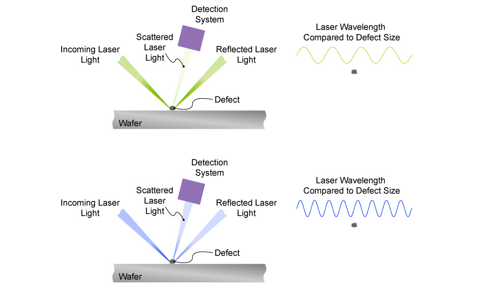
Shorter laser wavelengths are required to detect smaller defects because of the relationship between light scattering and defect size. Currently, 266 nm lasers are used for the most demanding wafer inspection tasks.
Two decades ago, when transistors were a comfortable 110 nm or larger, visible green lasers (532 nm) and ultraviolet (UV) lasers sufficed for defect detection. But shrinking circuit features have propelled the industry towards deep-ultraviolet (DUV) lasers.
Coherent met this challenge head-on with the introduction of our groundbreaking Azure laser in 2002. This laser utilizes Optically Pumped Semiconductor (OPS) technology to produce green output which is then frequency doubled into the DUV (266 nm).
The Azure delivers continuous wave (CW) output at a single, frequency-stabilized wavelength. Its combination of a narrow wavelength, high power, low noise, and extreme stability enables reliable detection of small defects at the speeds necessary for high-throughput semiconductor fabrication.
Coherent distinguishes itself with our ability to make high-power, deep UV lasers that offer exceptional lifetime and reliability. There are several reasons why we’re able to accomplish this.
First, we make our own non-linear crystals. Working in the deep UV demands extraordinarily high-quality crystals manufactured with tremendous precision. The only way we can obtain the quality level we need for our frequency doubling crystals is to make them ourselves.
Next, we employ our own patented PermAlign construction for the optical mounts within the laser itself. These mounts deliver exceptional long-term stability, which means that no adjustments will ever be required. PermAlign mounts allow us to hermetically seal the laser resonator. And this is key to preventing the ingress of any environmental contaminants which might impact laser performance. Plus, the lasers are originally assembled in cleanroom conditions using semi-automated methods to avoid any contamination at the outset. This also ensures a high degree of unit-to-unit consistency.

Go/No Go check for part conformance on an in-process wafer chuck.
Another requirement for wafer inspection is high speed motion and part handling mechanics, together with an extremely stable surface (to minimize measurement noise). We supply reaction bonded SiC (RBSiC) for stages and other tooling that deliver the unique mix of low thermal expansion (CTE), high strength, and high strength-to-weight ratio needed for the most demanding inspection systems.
Future Roadmap
As the semiconductor industry progresses towards even smaller nodes, the demands on inspection lasers become even more stringent. Fortunately, this aligns perfectly with our core strengths at Coherent. We maintain close collaboration with leading wafer fab equipment manufacturers, ensuring that our products not only meet, but anticipate, the needs of semiconductor manufacturing processes. Thus, Coherent empowers manufacturers to surmount the inspection challenges of today and tomorrow.
Learn more about Coherent Azure lasers.